Project AKO
HomeNews
AKO@sf.net
Overview
AKOI2C
AKONET
Components
Main Controller
Project AKO Photos
This page contains a variety of photos of the AKO system.AKO in Action (The Setup)
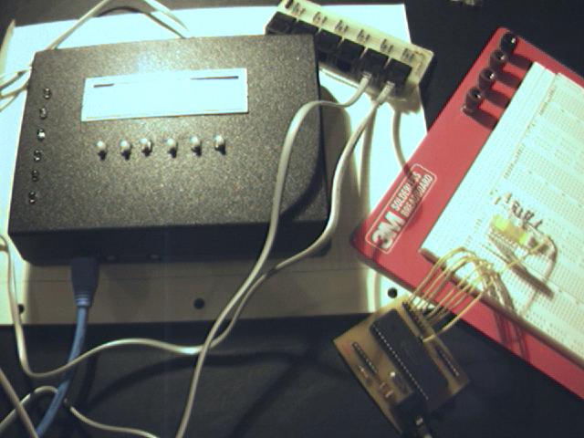
The above photo shows AKO about to give the demo in the video clip below. The black box on the left is the uCsimm based Main Control Board (MCB). Note the blue Ethernet cable coming out the bottom. Directly to the right of the MCB, at the top of the photo, you'll see a first version AKONET hub. The hub has the MCB and a digital I/O component plugged into it. The grey cable hooking everything up is standard flat satin phone cabling. At the bottom of the picture, a little right of center, is a digital I/O component. One of the ports on the DIO component is hooked up to a group of LED's on the big breadboard on the right of the photo.
AKO in Action (The Payoff)
Digial I/O Demo (696 kb MPEG)The MPEG movie linked above is the setup in the above picture doing some work. I'm telnet'd into the MCB from a-ko, running a program that simply counts up on one of the digital I/O component's ports. The LED's on the breadboard are there to let you watch it counting up. The program that the MCB is running is actually on an NFS mount on c-ko. The wonders of networking...
Outside the MCB
The MCB is a custom computer system that can be used as an AKO central controller. It is based on a uCsimm, and runs uClinux. It has a Dragonball EZ processor, 8 meg RAM, 2 meg Flash EEPROM, 10Base-T Ethernet, serial, AKONET, an alphanumeric LCD, and some switches and LED's.

Above is an outside shot of the front of the uCsimm based MCB.
There are 6 LED's along the side, 6 momentary push switches along the
middle, and a 2x20 alphanumeric LCD along the top. The MCB is
greeting everyone at SourceForge in this photo.

Above is a detail of the front side of the MCB. You can see the
10-BaseT Ethernet port, and a DB-9 serial port. The 10-BaseT obviously
allows for all kinds of network connectivity (like the telnet and NFS I used
in the above demo). The serial port is used mainly for debugging and
for uploading flash EEPROM images.

Above is a detail of the back side of the MCB. On the left is a DC
power connector. We've run the MCB off a 7.2V nicad pack for several
hours at a time. In the middle is an RJ-11 AKONET connector.

Above is a detail of the left side of the MCB. The only thing of
interest over here is the contrast adjustment for the LCD, which due to
bad workmanship on my part is exceptionally hard to turn.
Inside the MCB

A shot of opening up the MCB. The power regulators are conspicuous in the front of the shot.

Above is a shot of the lid of the MCB case, with all the switch and
LED connectors. Yes, that's solid wire. Huge mistake, but it
was the only thing I had when I wired it up late one Sunday night.
It's a pain to put back together. You can't really see it in this
picture, but there's huge globs of epoxy holding all the switches and
LED's in place. There's also massive amounts of electrical tape
holding the LCD panel in place.

This is a shot of the heart of the MCB. The power regulator board
is in the lower left. The uCsimm is mounted near the top of the
controller. The large DIP chip on the board is the AKOI2C I/O
coprocessor.

This is a close in shot showing the AKOI2C coprocessor, and all the glue
glue logic chips. The uCsimm is visible in the bottom of the photo.

Here's a shot of the uCsimm mounted in the MCB control board. This
is the side with the CPU, LAN, and memory chips.

Another shot of the uCsimm, this time from the other side. The AKOI2C
is in front of it. The wires connecting the AKOI2C to the RJ-11 AKONET
jack are in the extreme foreground.

Another shot of the control board, this time with the uCsimm removed.
The 10Base-T and DB-9 connectors are visible at the bottom of the photo.

Above is a shot of the underside of the MCB control board. The
SIMM socket for the uCsimm and the DIP socket for the AKOI2C are
conspicuously obvious. Note the blue trace wire on the right
side. A small design change to the board had to be made after it was
milled, because the LCD write cycle was unexpectedly bizarre. Chaulk
this up to bad research on my part.

A shot of the MCB, with just the power board and RJ-11 connector.
Components
Below are pictures of some of the components that are currently living at my apartment. Some of the cooler looking ones, like the mobile base unit, are currently living at Chris' house. I'll try to get some photos of them soon.Digital I/O

Above is a first generation digital I/O (DIO) component. The SIP sockets in groups of 8 provide access to the 24 I/O lines on it. The two SIP socket pair provide access to +5 and ground. The newer DIO components use a TQFP version of the PIC, and are much smaller. They also have a header for in-circuit programming of the PIC.

The trace side of the single-sided DIO board. You'll note it's a
fairly straightforward board.
Infrared Proximity Sensor

Above is an infrared proximity sensor component, minus the PIC microcontroller. The infrared LED and detector are seperate from the PCB, so that they may easily be placed in any orientation.

The trace side of the single sided proximity sensor component. This
board is even simpler than the DIO board. The socket in this board
had some corrosion on it and solder didn't stick very well, hence the
flux residue everywhere.
A Breadboarded Test Component

Above is a breadboarded component, which is currently being used to test the new AKOI2C device driver.
A Historical 16C64

The 16C64 in the above shot was one of two used in developing the original AKO components. We started using the 16F877 for components after the first semester of the project.
PC-AKO
The PC-AKO allows any PC with a bidirectional parallel port to communicate on an AKONET. This allows PC's to be used as the central controller. A USB PC adapter is in the works.

Above is first generation PC-AKO board. The big chip is essentially
the same AKOI2C
I/O coprocessor the MCB used. The difference is that the MCB version
had code to handle the LED's and switches, while the PC-AKO version has
code to handle the three LED status indicators. The DB-25 parallel
port connector is on the left, and the power and AKONET connections are at
the top. The three LED's are used as status indicators.
One LED is lit whenever there is activity on the AKONET.
The other two warn when the AKOI2C's internal buffer's have overflowed.
Again, the new generation PC-AKO's use a TQFP, are about the size of
DB-25 dongle, and have a header for in-circuit programming of the PIC.
The new generation also does not have a power regulator, requring another
power source to be located on the AKONET bus.

This is the trace side of the PC-AKO's single sided board.
AKONET Hub

Above is a top view of a first generation AKONET passive hub. The new generation have a power regulator section on the board, allowing the AKONET bus to be powered from the hub. The new generation is also double-sided, removing the need for all those jumpers you see on the board.

The hub from the front, looking into those RJ-11 jacks.
Some Real Computers
a-ko and c-ko were angry that there were a bunch of pictures of microcontrollers on the page, and no "real" computers. a-ko and c-ko are my desktop systems, and do the work like compiling device drivers, assembling firmware, and burning PIC's.a-ko

Above is a-ko, my main desktop system.
c-ko

Above is c-ko, which does a little bit of everything. c-ko took many trips up to school to help out during the senior design project.